Electron microscopy for particle size analysis
Electron microscopy is used in part as a particle size analysis technique that is either implemented as transmission electron microscopy or TEM, and scanning electron microscopy or SEM. The two techniques image samples, such as individual particles, dried from solution, and allow precise measurements of the samples’ geometric characteristics. For particles, these could include the diameter, shape, general surface properties, among other descriptors. In either case, of course, the researcher can take stunning micrographs of their samples.
Spectradyne’s fast and simple particle measurement systems
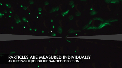
Spectradyne provides simple and inexpensive instrumentation that rapidly measures every particle individually, providing particle-by-particle sizing and accumulated statistics yielding concentration versus particle size. Spectradyne’s instruments provide a compelling and complementary technology to electron microscopy imaging.
Read about our microfluidics-based benchtop instrumentation.
Electron microscopy (TEM and SEM)
Electron microscopy, specifically transmission electron and scanning electron microscopy (TEM and SEM), are the gold standards for general nanoscale-sample characterization, including nanoparticle size and morphology analysis.
To prepare a sample for electron microscopy, the sample typically must be dry. For example, when studying a fluid sample containing nanoparticles, the sample would be dried from a few milliliters of the fluid. The dried sample is in some cases then coated with a nm-thick layer of conductive carbon or gold, to prevent spurious charging while viewing the sample. The dried and coated sample is then placed in the sample analysis chamber of the microscope; most commonly this is in vacuum, although more expensive modern electron microscopes allow sample examination in air.
The sample is then illuminated with a high energy beam of electrons generated by a cathode; the electrons can range in energy from a few kilovolts to a few hundred kilovolts, and are focused by coaxial magnets to a focus point 0.1 to 1 nm in diameter. This focus point is scanned over the sample in an SEM, while in a TEM the beam passes through the sample and the scattering occurs during the passage through the interior, after which scattered electrons are imaged on a charge-coupled detector (CCD). Either the scattered electrons, or in some cases the secondary electrons generated by the primary beam electrons, or both, are collected and projected into an imaging system. Very high resolution images of the sample, and in particular nanoscale particles, can be formed in this way, and analyzed with precision measurement tools calibrated on the microscope using calibration standards. An example is shown in the image to the right. In a TEM, it is even possible when viewing crystalline samples, to image the atoms that make up the sample, and from these images, determine the crystalline structure.
Using this imaging technique, particle diameters can be measured with great precision, and the geometric details of each particle are revealed in the images. By forming many images and using automated software, the size distribution of particles can be calculated and a concentration versus particle diameter can be calculated. An example is shown to the right, below the SEM image.
The sample preparation and sample imaging as well as image analysis are very time-consuming. TEMs and to a lesser extent SEMs are large, room-filling pieces of equipment that need special spaces with low vibration, low stray magnetic fields, and good temperature control. Using this method as a regular sample measurement technique is clearly prohibitive in terms of both cost and time. The data are typically used as an orthogonal verification of some of the other techniques discussed here.
Because of the expense and time-consuming nature of SEM and TEM analysis, researchers are always looking for alternative approaches, especially if they need data on a large population of samples. If the samples are nanoparticles suspended in fluid, the Spectradyne nCS1TM provides the next-best alternative to the electron microscopy gold standard: This unique microfluidic instrument detects each individual nanoparticle and measures its geometric volume, doing so in a few microseconds and thus allowing the measurement of thousands or hundreds of thousands of particles in a few minutes’ measuring time. The geometric volume of each particle can be converted to an equivalent diameter; the nCS1 can measure down to particle diameters of 30-40 nm and up to a few microns, depending on the specific microfluidic cartridge used for the analysis.
As a comparative example, the graph on the right shows results from three identical samples of urinary extracellular vesicles (EVs) measured in three different ways: Using the “gold standard” transmission electron microscopy (TEM: green line), using Spectradyne’s nCS1TM (nCS1: blue dots and line), and using nanoparticle tracking analysis (NTA: red line). The data show excellent quantitative agreement between TEM analysis and the results from the nCS1, but NTA fails quite badly at the smaller particle diameters, below about 150 nm in diameter.
Note that the nCS1TM data are taken in just a few minutes, with a total sample volume of 3 μL, using an instrument that costs a fraction of the cost of an SEM.

A typical image of nanoparticles taken with a scanning electron microscope (SEM).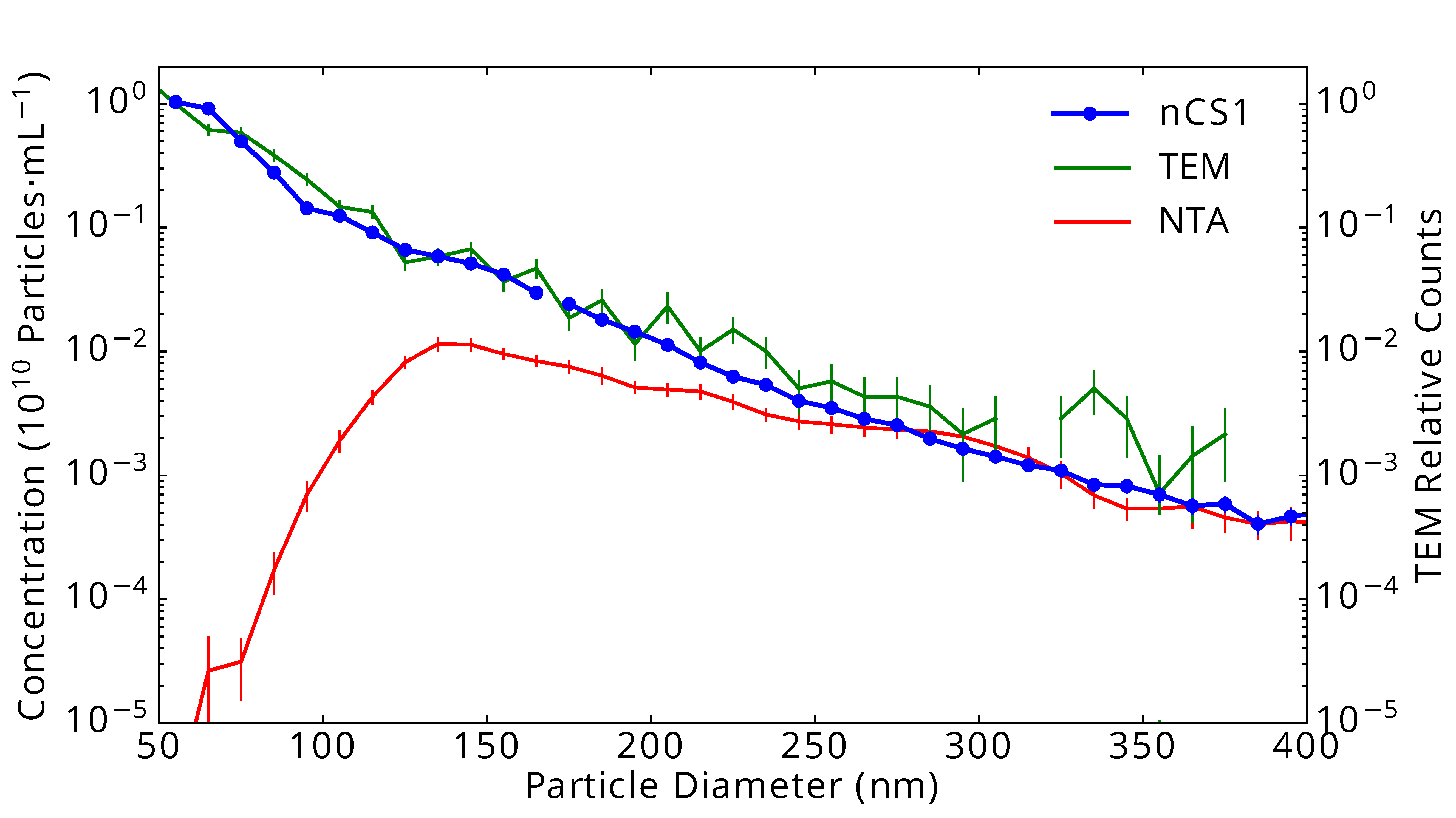
Urinary vesicles measured in three ways: Using “gold standard” transmission electron microscopy (TEM: green line), using Spectradyne’s nCS1TM (nCS1: blue dots and line), and using nanoparticle tracking analysis (NTA: red line).
The data show excellent agreement between TEM analysis and the results from the nCS1TM, but NTA fails quite badly at the smaller particle diameters, below about 150 nm in diameter. Vertical lines indicate statistical uncertainty in concentration.